A printed circuit board can look perfect on screen and still fail during production. A missing footprint detail can stop assembly. A wrong clearance can cause a short circuit. A poor layer stack can create signal problems that appear only after testing.
PCB design software helps engineers prevent these failures. It connects circuit diagrams, component placement, copper routing, mechanical checks, and manufacturing files.
But the most important feature is not automatic routing. It is how well the software keeps the electrical design, physical board, component data, and factory handoff in sync.
That distinction matters when choosing software. A hobby project, a small product team, and a high-speed electronics manufacturer do not need the same design environment.
What PCB design software must keep connected
A PCB project contains more than copper tracks and component outlines. It holds several linked forms of engineering information.
The schematic describes how components connect. The PCB layout shows where those components sit and how copper connects them. The component library links electrical symbols to physical footprints and, often, 3D models.
A reliable workflow keeps these parts aligned as the design changes.
Imagine an engineer replaces a voltage regulator with another part. The new component may have a different footprint, pin arrangement, or thermal pad. The engineer must update the schematic, check the footprint, review the board layout, and confirm that the new part meets the electrical needs.
If the software does not track these changes well, the board can contain errors even when its layout looks correct.
The core stages of a PCB project
| Stage | What engineers do | What can go wrong |
|---|---|---|
| Schematic capture | Draw components and electrical connections | Wrong pins, missing connections, unclear design intent |
| Component selection | Choose parts and assign symbols and footprints | Incorrect footprint, obsolete part, unavailable component |
| Board planning | Define board shape, layers, stackup, and placement | Mechanical clashes, poor layer choices, space problems |
| Component placement | Position parts on the board | Poor thermal layout, noise, difficult assembly |
| Routing | Connect pads with copper tracks and vias | Clearance errors, bad return paths, routing congestion |
| Design checks | Run electrical and physical rule checks | Unconnected nets, short circuits, rule violations |
| Manufacturing preparation | Create fabrication and assembly files | Missing drill data, wrong layer mapping, incomplete BOM |
These stages do not always happen in a strict sequence. Engineers often move between them as they refine the design.
The software choices that matter in practice
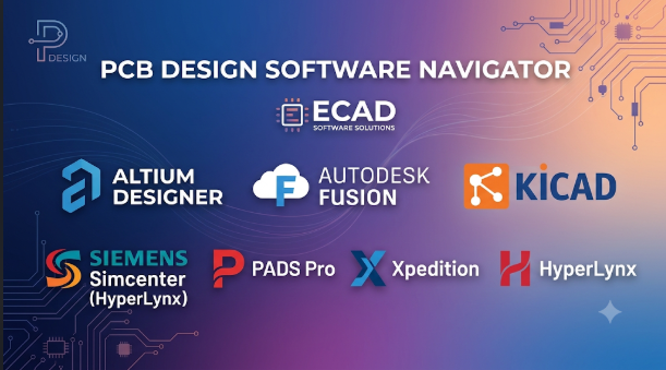
PCB design products range from open-source desktop tools to large enterprise engineering platforms. The right choice depends on board complexity, team size, collaboration needs, and manufacturing requirements.
Altium Designer: A connected design and release workflow
Altium Designer is a commercial PCB design environment that brings schematic capture, board layout, component data, and manufacturing preparation together.
One useful part of its workflow is the Output Job system. Engineers can define repeatable sets of outputs for fabrication, assembly, and documentation. They can also include validation reports such as electrical rule checks and design rule checks.
This matters when a company builds many boards. A team can reuse approved output settings rather than rebuilding manufacturing packages by hand for every project. Its documentation also describes controlled design releases and Workspace-hosted output jobs.
Altium is worth evaluating when a team wants a connected design environment and structured release process. Its wider collaboration and data management options should be reviewed against the company’s licensing and deployment needs.
The main consideration is the commercial commitment. Check the exact subscription, Workspace, server, and collaboration capabilities included in the proposed setup. Do not assume every data management feature comes with every license.
Cadence Allegro X: Constraint-driven design for demanding boards
Cadence Allegro X targets a wide range of PCB work, including complex and high-performance designs.
Its strength is the connection between layout and engineering constraints. Teams can define physical and electrical rules that guide routing and help control design behavior. This becomes important when a board has high-speed signals, dense routing, rigid-flex sections, or strict clearance requirements.
Cadence also connects PCB layout with schematic capture, in-design analysis, and data management. Its platform documentation describes ECAD-MCAD collaboration and integrations with analysis tools such as Sigrity and Clarity.
For large engineering teams, the Allegro X Collaboration Server can support project sharing, versioning, library management, and PLM connections. That can help control design data across teams.
The trade-off is implementation complexity. Buyers should map the required Allegro products, analysis options, libraries, and collaboration services before comparing license costs. A small board project may not need this depth.
Siemens Xpedition: Parallel engineering and manufacturing coordination
Siemens Xpedition is aimed at teams developing complex electronic products.
Its advanced offering combines routing automation, extended constraints, signal integrity verification, rigid-flex support, and manufacturing documentation. Siemens also describes real-time multi-user schematic work, which can help teams divide work without relying only on sequential file handoffs.
This is especially relevant when several engineers work on one product. The electrical design must stay aligned with mechanical packaging and manufacturing requirements. Xpedition’s ECAD-MCAD collaboration and BluePrint documentation workflows address that broader process.
Xpedition Standard and Advanced do not provide identical capability sets. Buyers should compare the exact tier against their needs for high-speed constraints, routing automation, concurrent design, and manufacturing preparation.
It is more suitable for teams with structured engineering workflows than for someone who only needs to lay out a simple hobby board.
Zuken CR-8000: Designing the whole electronic system
Zuken CR-8000 takes a system-level approach to PCB design.
It supports work that extends beyond a single board. Its tools address system architecture, multi-board design, mechanical integration, signal and power integrity, and IC package design.
This matters in products where several boards work together. Engineers may need to plan how boards connect, fit inside an enclosure, and share electrical or thermal loads. A design process focused on one PCB at a time can miss these system-level issues.
CR-8000 also includes capabilities for manufacturing preparation and engineering data management. Its architecture is relevant to organizations managing complex products and multiple design configurations.
The trade-off is the scope of the platform. A company should assess whether it needs system planning and multi-board coordination, or whether a conventional PCB workflow would be enough.
KiCad: A capable open-source route for PCB development
KiCad is a free, open-source EDA suite for schematic capture and PCB layout. It runs on Windows, macOS, and Linux.
It includes schematic and PCB editors, library tools, a 3D viewer, and manufacturing outputs. Its PCB editor supports design rule checks, interactive routing, differential pairs, and length tuning. It can also generate formats such as Gerber and IPC-2581.
KiCad is a strong option for independent engineers, education, prototypes, open hardware, and teams that want to avoid commercial license costs.
Its open-source model gives users control over their project files and software environment. But companies still need to manage component libraries, project reviews, backups, and approved manufacturing releases.
A business should also consider who will maintain shared libraries and support the design process. Free software does not mean free engineering time.
EasyEDA Pro: A browser-oriented path from design to board order
EasyEDA Pro offers schematic and PCB design through an online editor and desktop client.
Its workflow connects design work with component libraries and manufacturing services. This can be convenient for students, makers, and small teams that want to move from a schematic to a physical prototype without building a complex toolchain.
EasyEDA Pro supports PCB projects with or without an existing schematic. Its documentation covers board creation, design rules, libraries, and manufacturing exports. The platform also provides project and library features for its users.
Its close relationship with component and board services is a practical advantage for quick prototyping. However, teams should understand the service dependencies before adopting it for long-term product development.
Check how project data is stored, how designs can be exported, what happens when a project moves elsewhere, and whether the available manufacturing outputs meet your supplier’s requirements. Also review the differences between EasyEDA Standard and Pro rather than assuming they have the same features.
Autodesk Fusion Electronics: PCB design alongside mechanical product design
Autodesk Fusion includes an electronics workspace that connects schematic, 2D PCB, and 3D PCB documents.
That connection is useful when a board must fit inside a physical product. Engineers can work with the board’s shape and component models while considering the enclosure and other mechanical parts.
Autodesk’s documentation describes an electronics design document that manages the linked schematic, 2D board, and 3D board. It also explains how changes move between the associated design documents.
This makes Fusion relevant to product teams that already use its mechanical design environment. It can help reduce the gap between electrical and mechanical decisions.
However, it should not be treated as a direct replacement for every specialist enterprise PCB platform. Teams with demanding high-speed routing, advanced constraints, or large concurrent design workflows should test those requirements carefully.
Which tool fits which kind of team?
The products above serve overlapping but different needs. This summary can help narrow an initial shortlist.
| Team or project | Products worth evaluating | Main reason |
|---|---|---|
| Independent PCB designer | KiCad, EasyEDA Pro | Accessible design workflows and lower entry costs |
| Student or electronics learner | KiCad, EasyEDA Pro | Schematic and board design for learning and prototypes |
| Small product development team | Altium Designer, KiCad, Fusion Electronics | Connected design, collaboration, or mechanical integration |
| High-speed PCB engineering | Cadence Allegro X, Siemens Xpedition | Constraint-driven routing and signal integrity workflows |
| Large multi-board product | Zuken CR-8000, Siemens Xpedition, Cadence Allegro X | System planning, team coordination, and complex design management |
| Electronics and mechanical co-design | Autodesk Fusion, Altium Designer, Siemens Xpedition | Better coordination between board and enclosure design |
This is a starting point, not a universal ranking. The final choice depends on the exact board, team, and manufacturing process.
The component library problem deserves more attention
A PCB editor can only work with the component information it receives. A poor library can undermine an otherwise excellent design.
Each component may need several linked items:
- A schematic symbol that shows its electrical pins.
- A PCB footprint that defines pads and physical dimensions.
- A 3D model that helps check mechanical fit.
- A manufacturer part number and supplier details.
- Electrical and assembly properties used in reports and purchasing.
These items must agree.
A footprint with the wrong pad spacing can make a board impossible to assemble. A symbol with incorrect pin mapping can create a circuit error. A missing 3D model can hide a clash with an enclosure.
A company should decide who approves new library parts. It should also define how engineers handle obsolete components, alternate parts, and supplier changes.
For larger teams, a managed component library can reduce repeated work. It can also help prevent different engineers from creating separate versions of the same part.
Part availability is an engineering issue
A component may be electrically suitable but difficult to source. Its price, lead time, lifecycle status, and approved alternatives can affect the whole product.
Check whether the software can connect component information to supplier data. Then decide how often the team will review that information.
Do not rely on a library entry alone as proof that a part is available. Verify critical components with the manufacturer or authorized supplier before releasing a design.
Automatic routing cannot replace electrical judgment
Autorouting can help connect nets, but it does not understand every product requirement.
A router works within the rules and constraints supplied to it. If those rules are incomplete, the result may be electrically poor even when it passes basic design checks.
For example, a high-speed differential pair needs controlled spacing and length matching. A power circuit may need wide copper paths and careful thermal planning. A sensitive analog signal may need distance from noisy switching circuits.
These needs require engineering decisions before and during routing.
Important layout concerns include:
Signal integrity: Fast signals can suffer from reflections, crosstalk, and poor return paths. Routing rules and stackup choices affect their behavior.
Power integrity: Voltage drops and noise can affect components. Plane design, decoupling, and current paths need attention.
Thermal behavior: Power components generate heat. Placement, copper area, thermal vias, and airflow can affect temperature.
Electromagnetic compatibility: Board layout can influence emissions and susceptibility. Grounding, return paths, filtering, and enclosure design all matter.
Manufacturing limits: Track width, spacing, drill size, copper weight, and layer registration must fit the chosen fabricator’s process.
A software package may offer analysis features for some of these problems. Others may require separate specialist tools or external engineering review.
Manufacturing files are not just export buttons
A finished PCB project needs a controlled manufacturing package. The files must describe the board clearly enough for fabrication and assembly.
Common deliverables include:
- Gerber or another accepted fabrication data format.
- NC drill files for holes and vias.
- A board stackup and fabrication notes.
- A bill of materials.
- Component placement or pick-and-place files.
- Assembly drawings and polarity details.
- Test information where required.
Some manufacturers accept IPC-2581 or ODB++ as structured alternatives to separate files. The correct choice depends on the board house and its production workflow.
KiCad documents support for Gerber and IPC-2581 output. Altium’s Output Job documentation describes how teams can group fabrication, assembly, and validation outputs into reusable job files.
The key is consistency. A manufacturing package should come from one approved design revision. Do not send a new BOM with an older board layout.
A simple release check
Before sending files to a manufacturer, confirm:
- The schematic and PCB have no unresolved engineering changes.
- Electrical and design rule checks have been reviewed.
- The board outline and layer stackup match the fabrication plan.
- Drill files and copper layers use the correct settings.
- The BOM matches the approved component list.
- Placement files match the final board revision.
- The manufacturer has confirmed its required formats and specifications.
- The release package has a clear revision identifier.
This process helps prevent avoidable production delays.
What to test before selecting a PCB design platform
A short product demonstration rarely shows how software behaves with your real design data. A pilot project offers a more useful comparison.
Choose a board that reflects the work your team actually does. Include the parts, routing constraints, layer count, and mechanical limits that matter.
Then test these practical tasks:
- Import or create a real schematic.
- Add components from your current library.
- Replace a component with an approved alternative.
- Push schematic changes into the PCB layout.
- Define board stackup and design rules.
- Route critical nets with the required constraints.
- Run design rule checks and review the reports.
- Export fabrication and assembly files.
- Reopen the project and verify the released data.
- Exchange the board with your mechanical design workflow.
For a team project, also test permissions, concurrent editing, review comments, revision history, and library control.
Record how much setup the software needs. Note which tasks require separate tools or manual steps. These details often matter more than a polished product demonstration.
Questions to settle before paying for licenses
A PCB design tool becomes part of the product development process. The buying decision should cover more than editor features.
Ask vendors:
- Which schematic, layout, and analysis functions are included?
- Which advanced routing and simulation tools cost extra?
- Can the platform manage shared libraries and approved components?
- How does it handle project revisions and design releases?
- Can engineers work on the same project at the same time?
- Which MCAD and PLM systems can it connect to?
- What fabrication and assembly formats can it produce?
- Can the team use its existing design files?
- Where is project data stored, and who can access it?
- What support, training, and migration services are available?
Also ask for a demonstration using a representative board. A real design reveals gaps that a generic demo may not show.
The right PCB tool is the one that protects the handoff
For simple boards, KiCad or EasyEDA Pro may provide everything a designer needs. Fusion Electronics can make sense when mechanical product design is part of the same workflow. Altium Designer offers a connected design and release environment. Cadence Allegro X and Siemens Xpedition address demanding constraints and larger engineering teams. Zuken CR-8000 is worth considering when several boards and system-level decisions must stay coordinated.
The most important test is what happens after the layout looks complete. Can the team verify the design, manage its components, control revisions, and deliver correct manufacturing data?
Choose the software that supports those steps with the least risk and unnecessary complexity. A good PCB design is not finished when the last track is routed. It is finished when the approved design can be built, assembled, and checked as intended.





Leave a Reply
You must be logged in to post a comment.